AI Weirdness: the strange side of machine learning

Tag: science art

Total 76 Posts
(Untitled)

(Untitled)

This one looked to me like a line of people, standing at attention.  It’s actually an edge-on view of a comb-like grating structure, seen here as it passes between two rectangular alignment markers.  The people-like shape is due to the weird way the plasma etcher ate away the semiconductor,
(Untitled)

(Untitled)

Frostlike patterns emerge when acetone partially dissolves a plasticy layer of old photoresist.  This is the same sample as in my previous post [http://tmblr.co/ZP7VLs_nDmsM], which used to be covered in jagged black mountains made of plasma-damaged photoresist. Now the mountains are mostly dissolved away, except for
(Untitled)

(Untitled)

A strange miniature landscape, none of which is supposed to be there.  It’s quite small indeed - the pinnacles are each less than 1 micrometer tall, which means you’d need to stack a thousand of them on top of each other to equal one millimeter. This landscape is
(Untitled)

(Untitled)

Standing at the edge of the world. At microscopic scales, even a clean break isn’t very clean - this electron microscope picture is of the edge of a piece of glass, on which I had fabricated a long wall of semiconductor (the long columned wall you see at the
(Untitled)

(Untitled)

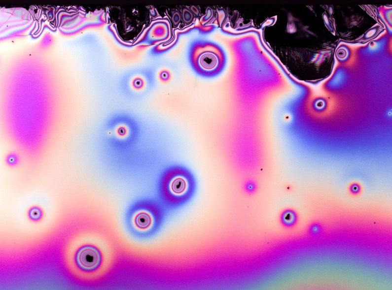
There are no dyes or pigments in this microscope image - it’s a thin clear film on a blank mirrorlike surface, and all the colors come from the interference of light waves.  It’s the same effect that produces the rainbow colors in thin soap bubbles, or on a
(Untitled)

(Untitled)

Another eerie example of nanoscale terrain echoing macroscale terrain - the cliff in this image is only about 1/200 the thickness of a typical human hair.  It’s been weathered away not by wind and rain, but by a blast of high-energy plasma.  The thick black mountainous layer is
(Untitled)

(Untitled)

The broken edge of a piece of semiconductor laser material, viewed at 2,402x under an electron microscope.  At this magnification, it’s clear that the edge isn’t cleanly broken at all, but has all sorts of furrows and ripples, all invisible to the naked eye, making it look
(Untitled)

(Untitled)

Even when working in the cleanroom, a little dust is hard to avoid.  This is a gallery of electron microscope pictures of dust specks I’ve encountered while making nanoscale devices in the UCSD Nano3 cleanrooms. Dust is made of a variety of materials - dead skin cells, tiny bits
(Untitled)

(Untitled)

I found an area of strange mesa-like structures on one of my samples - near this spot, the sample broke, scattering tiny fragments of glass and laser material across that part of the sample’s surface.  After I used high-energy plasma to etch most of the laser material away, the
(Untitled)

(Untitled)

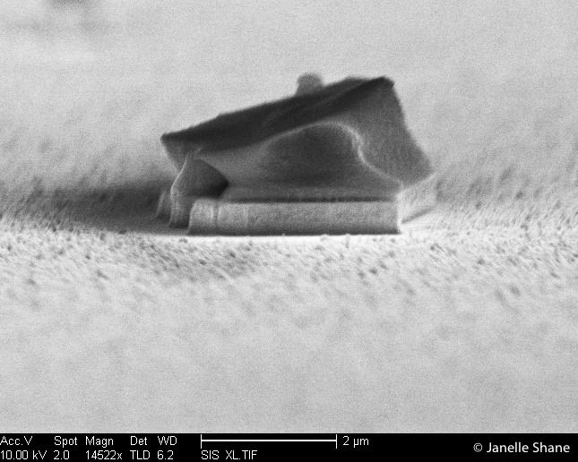
Nanosouffle?  This piece of dust appears to have partially deflated.  I’m not sure if it really did crumple, or if it’s just a trick of the angle.  The light-colored platform it’s sitting on is all semiconductor laser material, that the dust protected from the high-energy plasma that
You've successfully subscribed to AI Weirdness
Great! Next, complete checkout for full access to AI Weirdness
Welcome back! You've successfully signed in.
Unable to sign you in. Please try again.
Success! Your account is fully activated, you now have access to all content.
Error! Stripe checkout failed.
Success! Your billing info is updated.
Error! Billing info update failed.