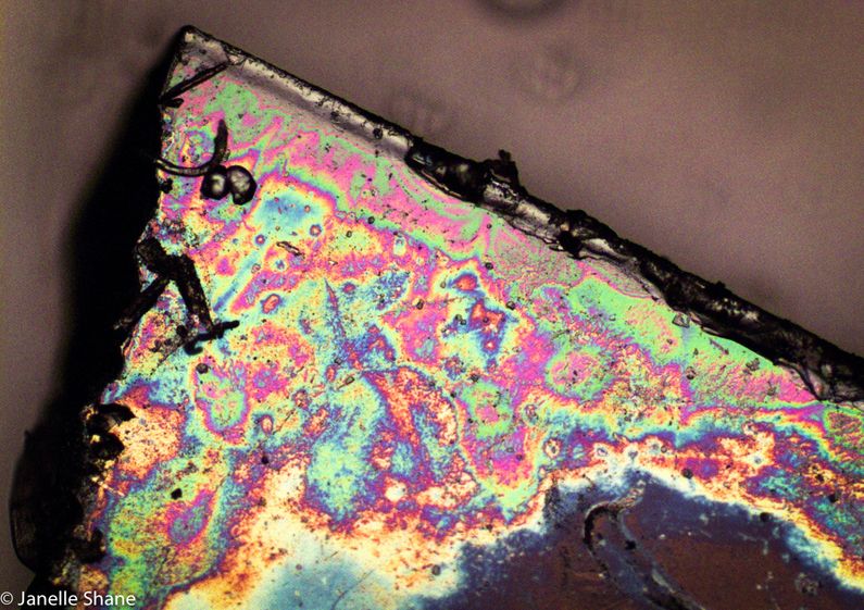
The cliffs of insanity? Rising an awe-inspiring 1.5 microns above the
wave-lashed sea (about 1/100 the thickness of a sheet of printer paper), these
cliffs were formed when high-energy plasma ate away a layer of semiconductor.
All that was left behind was this island, protected by a glassy
Pretty rainbow colors brought to you by the wave nature of light.
The phenomenon that made these wild colors out of a thin film of photoresist on
silicon is the same phenomenon that’s behind the rainbow colors of soap bubbles
and oily puddles. It’s also a more chaotic
A strange landscape with an even stranger sky.
This is a microscope view of the edge of a smooth chunk of silicon, coated with
a thin clear plasticy layer of photoresist. Just like the colors in a soap
bubble, this colorless thin layer produces rainbow colors due to the wave
It resembles a mushroom cloud, but in fact, it’s one of our microscopic
nanolasers, imaged under an electron microscope. These lasers are among the
smallest in the world, so small you could fit a billion of them on an iPhone
home button, small enough to one day fit easily
Strange formations caused when high-energy plasma from a reactive ion etcher
bombards semiconductor materials.
We use the reactive ion etcher to carve out microscopic optical devices, like
lasers and filters. Here, there’s no particular device that we were trying to
make - we were just testing to see if
The cliffs of fluffiness! Lashed by impossibly pointy nano-waves.
The fluffy stuff at the top is actually photoresist, a glassy substance that we
use to protect semiconductor from plasma bombardment when we’re doing our
etching. Here, the photoresist protected the semiconductor below it from being
etched away, making the
The color makeup of a fluorescent light, imaged through a spectrometer made of
folded paper and a chunk of DVD. You can print and fold your own for free
following the instructions here [http://publiclab.org/wiki/foldable-spec] (they
also have a kit [http://store.publiclab.org/products/foldable-mini-spectrometer]
, which
This one looked to me like a line of people, standing at attention. It’s
actually an edge-on view of a comb-like grating structure, seen here as it
passes between two rectangular alignment markers. The people-like shape is due
to the weird way the plasma etcher ate away the semiconductor,
A strange miniature landscape, none of which is supposed to be there. It’s
quite small indeed - the pinnacles are each less than 1 micrometer tall, which
means you’d need to stack a thousand of them on top of each other to equal one
millimeter.
This landscape is