(Untitled)


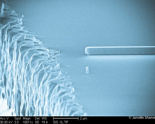
It’s a serene sight - a nicely formed wall of laser material (semiconductor InGaAsP, to be exact) stands on a smooth glassy plain.
I added the color - it’s not actually cold here. It’s inhospitable in a different sense, though: There isn’t any air. For the electron microscope to work, the sample needs to be in a vacuum chamber.
The only obvious defect to this nicely-etched sample is a small pillar, probably also of laser material, which has appeared for reasons of its own but luckily stands at a respectful distance from the wall I made. It’s far enough away that its presence won’t interfere with my experiments. It seems to merely observe.
If the little nanopillarguy (1 micrometer high) walks to the right at a proportional human walking speed, it would take about an hour of walking to reach the other end of the wall. (a 1m high human walks at 5km/hr, so a 1 micrometer high nanoguy would walk at 5mm/hr). Along the way they would pass giant letters the size of city blocks saying “1S200” (I label my walls!)
If the little nanoguy walks to the left, the results are much more immediate: falling off the immense cliff that is the edge of my chip. If the nanoguy were scaled up to the size of a human, the cliff would be 1km high (about 3300 feet), rivaling the height of the highest cliffs on Earth. At the bottom is a vast sea of black cratered carbon tape (used to make a good conductive contact between my chip and the microscope mount). Beyond that, even I get lost.
